20+ flip flop block diagram
Input transducer 3Formatter 4. It contains 20 pins which have three-state output.
1
20 Filter Circuits 9 Founder Speaks 3 GATE Questions and Answers 1 Integrated Circuits 7 Interview 8 Introduction to Electronics 1 JK Flip Flop 3 Logic circuits 1 Logic Gates and Boolean Algebra 10 Long Questions and Answers 3 MCQ 3.
. Array Multiplier in Digital Logic. 2 to 4 Decoder in Verilog HDL. Well also write the testbenches and generate the final RTL schematics and simulation waveforms for each flip-flop.
Pinning information 51 Pinning Remark. When you press a push button even. Each flip Flop has different input.
20 LED related 3 Light Related 14. Flip-flop types their Conversion and Applications. Fig1 shows the basic block diagram of a Digital Communication System.
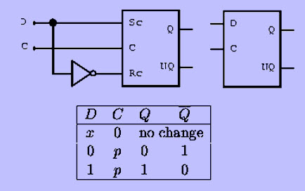
In the block diagramQ of RS Flip flop is connected no whereI think it must be connected to the the discharge transistorPlease get it corrected. Output port 1 register. The 555 timer IC is an integral part of electronics projects.
A 85C P. It determines the pulse width of the output 5 Voltage I. The Block diagram of the T flip-flop is given below where T defines the Toggle input and CLK defines the clock signal input.
We can construct the T flip-flop by making changes in the JK flip-flop. The counter is a digital sequential circuit and here it is a 4 bit counter. The RF input of the.
FUNCTIONAL BLOCK DIAGRAM R ENVELOPE. 20 19 22 21 24 23. Output port 0 register Table 8.
Join us at AutoSens Brussels. Onsemi as the lead sponsor of this event will showcase its intelligent sensing solutions for ADAS autonomous driving in-cabin viewing and LiDAR applicationsDont miss the chance to attend our keynote and meet with our experts to find the right solution for your design challenges. Block Diagram of Digital Communication System.
In electronics a flip-flop or latch is a circuit that has two stable states and can be used to store state information a bistable multivibratorThe circuit can be made to change state by signals applied to one or more control inputs and will have one or two outputs. 20 dBm 054. All IOs are set to inputs at reset.
Block diagram of design requirements. NAME Control Controls the threshold and trigger levels. Sequential logic functions such as Flip-Flop and Latches Qualification and Class-B Support AEC-Q100 Grade 1 -40ºC to 125ºC Class-B safety library IEC 60730 future Debugger Development Support Two-pin Serial Wire Debug SWD programming and debugging interface Packages 1 Type VQFN TQFP SSOP WLCSP.
Learn all about Function Block Diagram FBD the official PLC programming language described in IEC 61131-3. Lets write the VHDL code for flip-flops using behavioral architecture. SAM L10L11 Family Ultra Low-Power 32-bit Cortex-M23 MCUs with TrustZone Crypto and Enhanced PTC Features Operating Conditions.
Basic block diagram for PLA. Following Truth table will be helpful in understanding function on no of inputs-. These will be the first sequential circuits that we code in this course on VHDL.
162V to 363V -40ºC to 125ºC DC to 32 MHz. In this figure the different functional elements are represented by blocks. It is the basic storage element in sequential logicFlip-flops and latches are fundamental building blocks of digital.
In turn reads from th is register reflect the value that is in the flip-flop controlling the output selection not the actual pin value. Event is held on the flip-flop until a reset pulse is applied. Deviation from output at 25C.
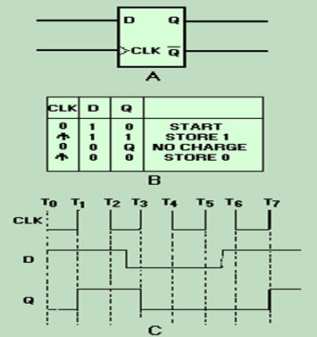
Synchronous Sequential Circuits in Digital Logic. The negative edge D flip-flop can be represented with a triangle and a bubble at the clock end of the D flip-flop block diagram. Block Diagram of Digital Communication System The essential components of a digital communication system are.
Many call this a flip-flop function. 10 Stunning Structures With Gorgeous Inner Courtyards House design with center courtyard see description you center courtyard house plans homedesignpictures 49577 center courtyard home plans timeless ranch design with glass facade 58 most sensational interior courtyard garden. We will code all the flip-flops D SR JK and T using the behavioral modeling method of VHDL.
The T flip-flop has only one input which is constructed by connecting the input of JK flip-flop. Flip-flop types their Conversion and Applications. All the flip-flops are mainly controllable by the clock and enable pin.
Discover all the collections by Givenchy for women men kids and browse the maisons history and heritage. Negative Edge Triggered D flip flop Circuit Diagram. Full Adder using Verilog HDL.
The project was designed by HYLA Architects and is located in Singapore. An open collector is a common type of output found on many integrated circuits IC which behaves like a switch that is either connected to ground or disconnectedInstead of outputting a signal of a specific voltage or current the output signal is applied to the base of an internal NPN transistor whose collector is externalized open on a pin of the IC. A complete tutorial of 555 Timer IC with its block diagram working of SENE 555 TimerPin Configuration and pin out diagram Download 555 data sheet.
T Flip Flop Circuit. These provide time delays as an oscillator and as a flip-flop element among other applications. As one of the inputs on the AND function is Q1 which also acts the output for the whole block.
This single input is called T. Be it a simple project involving a single 8-bit micro-controller and some peripherals or a complex one involving system on chips SoCs 555 timer working is involved. Q1 will remember that at some point S1 was true.
ADL5904 is dc-coupled allowing operation.

A Simple Bang Bang Loop Using A Flip Flop For A Phase Detector To Lock Download Scientific Diagram

A Conceptual Block Diagram Of A Non Volatile Flip Flop And B Download Scientific Diagram

Clocked T Flip Flop A Characteristic Table B Logic Circuits C Download Scientific Diagram

4 Major Types Of Flip Flop Circuits Edifythefacts
T Flip Flop

Clocked T Flip Flop A Characteristic Table B Logic Circuits C Download Scientific Diagram

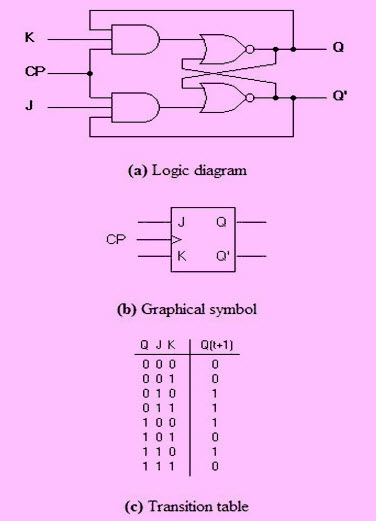
Logic Diagram Of J K Flip Flop Download Scientific Diagram

Block Diagram Of The Flip Flop Circuit Download Scientific Diagram
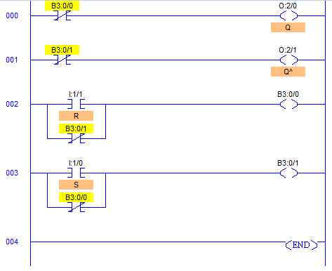
Plc Program To Implement Sr Flip Flop Sanfoundry
1
Flip Flop Circuit Types And Its Applications
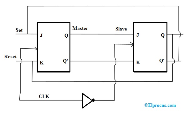
What Is A Master Slave Flip Flop Circuit Diagram And Its Working
Flip Flop Circuit Types And Its Applications

Quasi Static Negative Edge Triggered D Flip Flop Circuit Layout A Download Scientific Diagram
Test Circuit Schematic For Three Tag Flip Flops Each D Type Flip Flop Download Scientific Diagram
1
Flip Flop Circuit Types And Its Applications